

")

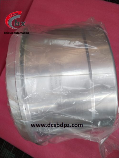
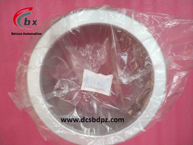
AMAT 0021-53986 Lower shielding cover
Specific parameters
Applicable wafer size: Supports 300mm wafers
Material: Made of copper or stainless steel to meet the requirements of corrosion resistance and thermal conductivity (refer to the product description of the same series).
Surface treatment: Silver plating or coating treatment (such as Clean Coat) to enhance corrosion resistance and reduce particle contamination.
Structural design: Modular design, easy to install and maintain, may include labyrinth pipes or heat dissipation structures.
Working temperature: Suitable for high temperature environments (such as plasma environments in etching processes).
Product Performance
High temperature resistance and corrosion resistance: Materials and surface treatment techniques enable it to withstand long-term corrosion from high temperatures (such as hundreds of degrees Celsius in plasma processes) and corrosive gases (such as fluorine based etchants).
Precision adaptation: Precise coordination with equipment chambers can ensure uniform distribution of process gases, reduce edge effects, and improve the consistency of wafer processing.
Low particle release: The surface treatment process reduces the risk of particle detachment and meets the strict cleanliness requirements of semiconductor manufacturing.
Long life design: By optimizing materials and strengthening structures, frequent replacement needs are reduced and maintenance costs are lowered.
application area
Semiconductor etching process: In plasma etching equipment, the bottom structure of the chamber is protected from high-energy ion bombardment, while assisting gas flow guidance.
Thin film deposition process: used in physical vapor deposition (PVD) or chemical vapor deposition (CVD) equipment to prevent deposition materials from adhering to non target areas and ensure film uniformity.
Advanced packaging and 3D NAND manufacturing: providing precise physical barriers in processes such as hybrid bonding and step etching, supporting the formation of high aspect ratio structures.
Display panel and solar cell production: applied to flat panel display or photovoltaic cell manufacturing equipment to protect key components from process environmental impacts.


There are no reviews yet.